Taima-Sohel Laboratory, Nanomaterials Research Institute, Kanazawa Univ.
金沢大学 ナノマテリアル研究所 當摩・ソヘル研究室
EQUIPMENTS
當摩研究室の実験機器・測定装置
薄膜太陽電池作製のための設備たちです。

グローブボックス
glove box

グローブボックスは、不活性ガス(窒素)で満たされた密閉空間で、酸素や水分に敏感な材料の取り扱いに使用されます。ペロブスカイトのように水分や酸素で劣化しやすい材料の成膜や処理に不可欠です。
A glove box is a sealed chamber filled with an inert gas (nitrogen) and is used for handling materials that are sensitive to oxygen and moisture. It is essential for fabricating and processing perovskite solar cells, which degrade easily in the presence of water and oxygen.
クリーンルーム
clean room

クリーンルームは、空気中の塵や微粒子を極限まで抑えた環境で、半導体や薄膜太陽電池の製造に使用されます。デバイスの成膜時に異物混入を防ぎ、均一な膜質を確保するために重要です。
A clean room is an environment with extremely low levels of airborne dust and particles, used in semiconductor and thin-film solar cell fabrication. It is crucial for ensuring uniform film quality and preventing contamination during the fabrication of devices.
金属蒸着装置
metal evaporation chamber

金属蒸着装置は真空中で金属や無機物を加熱・蒸発させ、基板�上に薄膜として堆積させる装置です。ペロブスカイト太陽電池では、電極(Au、Ag)やパッシベーション層(CuI、MoOxなど)の形成に使用され、均一に材料を製膜することができます。
A metal evaporation chamber can heat and evaporate metals and inorganic materials in a vacuum, depositing them as thin films on a substrate. In PSCs, it is used to form electrodes (Au, Ag, etc) and passivation layer ( MoOx, CuI etc).
スピンコーター
spin coater

スピンコーターは、基板上に液体材料を滴下し、高速回転させて均一な薄膜を形成する装置です。ペロブスカイトや輸送層の成膜に使用されます。
A spin coater is a device that dispenses liquid material onto a substrate and rapidly spins it to form a uniform thin film. It is commonly used for depositing active layers and transport layers in perovskite solar cells.
スパッタ装置
spatter machine
スパッタ装置は、プラズマを利用してタ�ーゲット材料を原子・イオンレベルで叩き出し、基板上に薄膜を形成する装置です。透明導電膜(ITO, AZO など)や金属電極の成膜に使用され、高密度で均一な膜を作ることができます。
A sputtering system uses plasma to eject atoms or ions from a target material, depositing them as a thin film on a substrate. It is used for forming transparent conductive films (ITO, AZO etc.) and metal electrodes, enabling the fabrication of high-density and uniform films.
ペロブスカイトチャンバー
perovskite chamber

ペロブスカイトチャンバーは、蒸着ペロブスカイトを含め、ペロブスカイト層の成膜を最適な環境で行うための専用チャンバーです。湿度や酸素の影響を抑えながら成膜できるため、膜の均一性や結晶性を向上させることができます。
A perovskite chamber is a specialized chamber designed for optimal deposition of perovskite layers, including evaporated perovskites. It minimizes the effects of humidity and oxygen during the deposition process, improving film uniformity and crystallinity.
有機グラッドチャンバー
organic GLAD chamber

グラッドチャンバーは、成膜時の蒸着角度を調整し、ナノ構造を制御できる装置で、主に有機材料の蒸着に使用されます。
A GLAD chamber is a device that can adjust the deposition angle during film formation and control nanostructures, and is primarily used for the deposition of organic materials.
レーザースクライバー
LASER scriber

レーザースクライバーは、高精度なレーザーを用いて薄膜を選択的に除去し、微細なパターンを形成する装置です。電極パターン作製や、セルの直列接続を行いモジュールを作製するために使用します。
A laser scriber is a device that uses a high-precision laser to selectively remove thin films and form fine patterns. It is used to create electrode patterns and to connect cells in series to create modules.
電極プリンター
electrode printer

電極プリンターは、印刷で電極を基板上にパターン形成する装置です。大面積デバイスの製造やフレキシブルデバイスの作製に利用され、低コストでスケーラブルな製造プロセスの実現に貢献します。
An electrode printer is a device that patterns electrodes on a substrate by printing. It is used for manufacturing large-area devices and fabricating flexible devices, contributing to the realization of low-cost and scalable manufacturing processes.
プラズマクリーナー・UVクリーナー
plasma cleaner/UV cleaner
クリーナーは、デバイスに使う基板の表面に付着した有機汚染物質を分解・除去したり、表面処理をするための装置です。 親水性の向上や表面エネルギーの向上を行い、製膜の補助をします。
Cleaner is used to decompose and remove organic contaminants adhering to the surface of substrates used in devices, and also to perform surface treatment. It improves hydrophilicity and surface energy and assists in film formation.
ソーラーシミュレーター
solar simulator

ソーラーシミュレーターは、太陽光を模擬する光源を用いて太陽電池の発電特性を評価する装置です。AM1.5Gスペクトルに基づいた��照射を行い、太陽電池の効率(変換効率、J-V特性など)を測定する際に使用されます。
A solar simulator is a device that uses a light source to simulate sunlight for evaluating the power generation characteristics of solar cells. It provides illumination based on the AM1.5G spectrum and is used to measure the efficiency (e.g., power conversion efficiency, J-V characteristics) of solar cells.
iPCE測定装置
incident photon-to-current efficiency measurement

iPCE(外部量子効率、EQE)測定装置は、特定の波長の光を照射し、それに対する太陽電池の電流応答を測定する装置です。光吸収特性、キャリア生成・収集効率、波長ごとの変換効率を解析し、デバイス性能の評価や材料設計に役立ちます。
An iPCE measurement system irradiates a solar cell with light at specific wavelengths and measures its current response. It is used to analyze light absorption properties, carrier generation/collection efficiency, and wavelength-dependent conversion efficiency, aiding in device evaluation and material design.
蛍光分析装置
Photoluminescence measurement system

蛍光分析装置は、材料が光を吸収した後に再放出する蛍光を測定し、発光特性や電子状態を解析する装置です。定性分析のほか、再結合特性や欠陥密度の評価、キャリア寿命の測定に使用され、デバイス性能の向上に役立ちます。
PL measurement system analyzes optical and electronic properties by irradiating a sample with light and measuring its emission spectrum. In addition to qualitative analysis, it is used to evaluate recombination properties and defect density, and to measure carrier life, which is useful for improving device performance.
原子間力顕微鏡
Atomic Force Microscopy (AFM)

AFMは、探針を試料表面に近づけて原子間の相互作用力を測定し、ナノスケールの表面形状や粗さを可視化する装置です。
AFM is a device to visualize nanoscale surface topography and roughness by measuring the interaction forces between atoms by bringing a probe close to the sample surface.
膜厚計
surface profiler

膜厚計は、針でたどることで薄膜の厚さを測定する装置です。膜厚はデバイスの性能に大きく影響します。
A film thickness gauge is a device that measures the thickness of a thin film by tracing it with a needle. Film thickness greatly affects device performance.
顕微鏡
microscopy

顕微鏡は、光学レンズや電子ビームを用いて試料を拡大観察する装置です。膜の欠陥やパターンの確認による微細構造の解析などに使用し、デバイスの品質評価に役立ちます。
A microscope is a device that uses optical lenses and electron beams to magnify and observe a sample. It is used to analyze microstructures by checking film defects and patterns, and is useful for device quality evaluation.
紫外・可視分光光度計
UV-vis spectrophotometer

UV-vis分光光度計は、紫外線から可視光領域の光の吸収スペクトルを測定する装置です。太陽電池デバイスの活性層や輸送層の光吸収特性やバンドギャップを評価し、光電変換効率向上のための材料設計に活用されます。
UV-vis spectrophotometer is a device to measure the absorption spectrum of light in the UV to visible light region. It is used to evaluate the light absorption characteristics and band gap of the active and transport layers of solar cell devices, and to design materials to improve photoelectric conversion efficiency.
環境試験装置
damp heat testing equipment

環境試験装置は、温度、湿度、ガス雰囲気などの環境条件を制御しながら試料の特性を測定する装置です。太陽電池の安定性試験に用いられ、熱・湿度・酸素・光照射による劣化の影響を評価し、長寿命化のための材料開発に貢献します。
An environmental test equipment controls conditions such as temperature, humidity, and gas atmosphere while measuring sample properties. It is used for stability testing, evaluating degradation effects due to heat, humidity, oxygen, and light exposure, contributing to the development of long-lasting materials.
X線結晶構造解析装置
X-ray Diffraction (XRD)

XRDは、X線を試料に照射し、回折パターンを解析することで結晶構造を評価する装置です。結晶相の同定、結晶性の評価、結晶粒サイズの推定、結晶の配向性の解析などに使用されます。
XRD is a device to evaluate crystal structure by irradiating X-rays to a sample and analyzing the diffraction pattern. It is used to identify crystalline phases, evaluate crystallinity, estimate crystal grain size, and analyze crystal orientation.
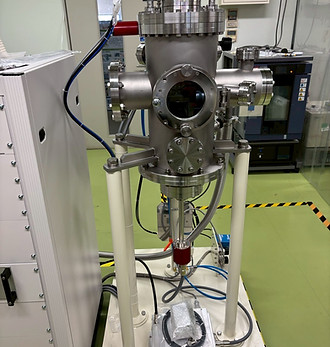
X線光電子分光分析装置
X-ray Photoelectron Spectroscopy (XPS)
.jpg)
XPSは、X線を試料に照射し、放出される光電子のエネルギーを測定することで、元素組成や化学結合状態を分析する装置です。表面の化学組成、酸化状態、不純物の分析に使用され、材料の安定性や劣化メカニズムの解明に役立ちます。
XPS can analyze elemental composition and chemical bonding states by irradiating a sample with X-rays and measuring the energy of the emitted photoelectrons. It is used to analyze the chemical composition, oxidation state, and impurities on surfaces, helping to elucidate the stability and degradation mechanisms of materials.
走査型電子顕微鏡(EDX付)
Scanning Electron Microscopy (SEM-EDX)

SEMは、電子ビームを試料に照射し、表面の微細構造を高倍率で観察する装置です。膜の形態、粒径、膜の均一性、層構造の断面解析に使用されます。EDXを組み合わせて試料にX線を照射し、元素組成を特定できます。
SEM is an instrument that irradiates an electron beam onto a sample to observe its surface microstructure at high magnification. It is used for cross-sectional analysis of film morphology, grain size, film uniformity, and layer structure; EDX allows the sample to be irradiated with X-rays to determine elemental composition.